- 您现在的位置:买卖IC网 > Sheet目录250 > SFCF4096H4BK2SA-I-QT-553-SMA (Swissbit NA Inc)FLASH SLC UDMA/MDMA/PIO 4G
�� �
�
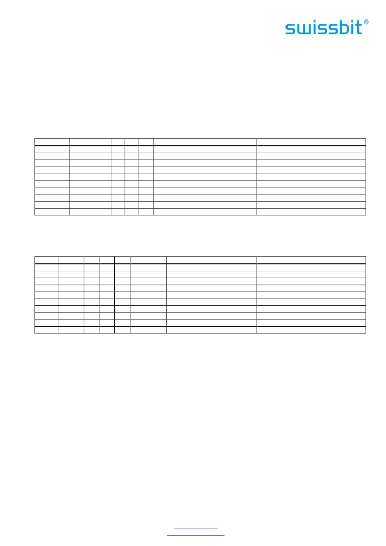
�8.4� I/O� Primary� and� Secondary� Address� Configurations�
�When� the� system� decodes� the� Primary� and� Secondary� Address� Configurations,� the� registers� are� accessed� in� the�
��As� for� the� Memory� Mapped� Addressing,� register� 0� is� accessed� with� –� CE1� Low� and� –CE2� Low� (and� A0� don’t� Care)� as� a�
�Word� register� on� the� combined� Odd� and� Even� Data� Bus� (D15� to� D0).� This� register� may� also� be� accessed� with� –� CE1�
�Low� and� –� CE2� High,� by� a� pair� of� Byte� accesses� to� offset� 0.� The� address� space� of� this� Word� register� overlaps� the�
�address� space� of� the� Error� and� Feature� Byte-wide� registers� at� offset� 1.� When� accessed� twice� as� Byte� register� with� –�
�CE1� Low,� the� first� Byte� is� the� even� Byte� of� the� Word� and� the� second� is� the� odd� Byte.� A� Byte� access� to� register� 0� with�
�–� CE1� High� and� –� CE2� Low� accesses� the� error� (read)� or� feature� (write)� register.�
�Table� 46:� Primary� and� Secondary� I/O� Decoding�
�-� REG�
�0�
�0�
�0�
�0�
�0�
�0�
�0�
�0�
�0�
�0�
�A9� to� A4�
�1F(17)h�
�1F(17)h�
�1F(17)h�
�1F(17)h�
�1F(17)h�
�1F(17)h�
�1F(17)h�
�1F(17)h�
�3F(37)h�
�3F(37)h�
�A3�
�0�
�0�
�0�
�0�
�0�
�0�
�0�
�0�
�0�
�0�
�A2�
�0�
�0�
�0�
�0�
�1�
�1�
�1�
�1�
�1�
�1�
�A1�
�0�
�0�
�1�
�1�
�0�
�0�
�1�
�1�
�1�
�1�
�A0�
�0�
�1�
�0�
�1�
�0�
�1�
�0�
�1�
�0�
�1�
�-� IORD=0�
�Even� Data� Register�
�Error� Register�
�Sector� Count� Register�
�Sector� Number� Register�
�Cylinder� Low� Register�
�Cylinder� High� Register�
�Select� Card/Head� Register�
�Status� Register�
�Alternate� Status� Register�
�Drive� Address� Register�
�-� IOWR=0�
�Even� Data� Register�
�Feature� Register�
�Sector� Count� Register�
�Sector� Number� Register�
�Cylinder� Low� Register�
�Cylinder� High� Register�
�Select� Card/Head� Register�
�Command� Register�
�Device� Control� Register�
�Reserved�
�8.5� True� IDE� Mode� Addressing�
�When� the� Card� is� configured� in� the� True� IDE� Mode,� the� I/O� decoding� is� as� shown� in� Table� 47� .�
�Table� 47:� True� IDE� Mode� I/O� Decoding�
�-� CS1�
�1�
�1�
�1�
�1�
�1�
�1�
�1�
�1�
�1�
�0�
�-� CS0�
�0�
�1�
�0�
�0�
�0�
�0�
�0�
�0�
�0�
�1�
�A2�
�0�
�X�
�0�
�0�
�0�
�1�
�1�
�1�
�1�
�1�
�A1�
�0�
�X�
�0�
�1�
�1�
�0�
�0�
�1�
�1�
�1�
�A0�
�0�
�X�
�1�
�0�
�1�
�0�
�1�
�0�
�1�
�0�
�-DMACK�
�1�
�0�
�1�
�1�
�1�
�1�
�1�
�1�
�1�
�1�
�-� IORD=0�
�PIO� RD� Data�
�DMA� RD� Data�
�Error� Register�
�Sector� Count�
�Sector� No.�
�Cylinder� Low�
�Cylinder� High�
�Select� Card/Head�
�Status�
�Alt� Status�
�-� IOWR=0�
�PIO� WR� Data�
�DMA� WR� Data�
�Features�
�Sector� Count�
�Sector� No.�
�Cylinder� Low�
�Cylinder� High�
�Select� Card/Head�
�Command�
�Control� Register�
�Swissbit� AG�
�Industriestrasse� 4�
�Swissbit� reserves� the� right� to� change� products� or� specifications� without� notice.�
�Revision:� 1.51�
�CH-9552� Bronschhofen�
�Switzerland�
�www.swissbit.com�
�industrial@swissbit.com�
�C-300_data_sheet_CF-HxBK_Rev151.doc�
�Page� 53� of� 99�
�发布紧急采购,3分钟左右您将得到回复。
相关PDF资料
SFCF64GBH2BU4TO-I-NU-517-STD
FLASH SLC UDMA/MDMA/PIO 64GB
SFN08B4702CBQLF7
RES ARRAY 47K OHM 7 RES 8-DFN
SFP1050-12BG
FRONT END AC/DC 1050W 12V
SFP450-12BG
PWR SUP 450W 12V 36.6A W/STANDBY
SFSD1024N1BN1TO-I-DF-151-STD
FLASH MICRO SD CARD IND S-200 1G
SFSD2048L1BN2TO-I-DF-151-STD
FLASH SECURE DGTL CARD SD 2G
SFSD4096L1BN2TO-I-Q2-141-STD
FLASH SECURE DGTL CARD SDHC 4G
SFSD8192N1BW1MT-E-QG-111-STD
FLASH MICRO SD 8GB EXT TEMP
相关代理商/技术参数
SFCF64GBH2BU4TO-C-NU-527-STD
制造商:SWISSBIT 功能描述:CFC C-440 DENSITY COMMERCIAL - Trays 制造商:SWISSBIT NA INC 功能描述:FLASH
SFCF64GBH2BU4TO-I-NU-517-STD
功能描述:FLASH SLC UDMA/MDMA/PIO 64GB RoHS:是 类别:存储卡,模块 >> 存储器,PC 卡 系列:C-440 标准包装:30 系列:- 存储容量:8GB 存储器类型:存储卡 - Extreme III SD?
SFCF64GBH2BU4TO-I-NU-527-STD
制造商:SWISSBIT 功能描述:CFC C-440 DENSITY INDUSTRIAL - Trays 制造商:SWISSBIT NA INC 功能描述:FLASH CARD 64GB IND C-440 制造商:Swissbit 功能描述:Memory Cards 64GB IND COMPACT FLASH SLC NAND C440
SFCF8192H1BO2TO-C-Q1-523-SMA
制造商:SWISSBIT NA INC 功能描述:FLASH
SFCF8192H1BO2TO-C-Q1-533-ZP1
制造商:SWISSBIT NA INC 功能描述:FLASH
SFCF8192H1BO2TO-C-Q1-543-SMA
制造商:SWISSBIT NA INC 功能描述:FLASH
SFCF8192H1BO2TOIQ1523SMA
制造商:Swissbit 功能描述:Flash Card 8G-Byte 3.3V/5V CompactFlash 50-Pin
SFCF8192H1BO2TO-I-Q1-523-SMA
功能描述:FLASH SLC UDMA/MDMA/PIO 8G RoHS:是 类别:存储卡,模块 >> 存储器,PC 卡 系列:C-320 标准包装:30 系列:- 存储容量:8GB 存储器类型:存储卡 - Extreme III SD?